FPGA + Zynq for Graphic Display Circuit
Introduction
This post documents the implementation steps described from Chapter 9 onward in the referenced book
reference-book It details the process of creating an HDMI graphic display IP using Vivado.
Environment
- FPGA: Xilinx Zybo Z7-20
- OS: WSL2 Ubuntu 20.04
- Development Environment: Vivado ML edition 2022.1 (Linux)
Objective
Develop an IP block in Vivado using HDL to output graphics via HDMI.
The IP block meets the following requirements:
- Display an image stored in DDR3 memory.
- VGA resolution (with future plans for extension).
- 24-bit RGB color.
- Controllable as an IP block from the Zynq.
- Pixel display address controlled via GPIO from the Zynq.
After developing the graphic display IP, integrate it with a bit-block drawing circuit created using Vitis HLS.
AXI Bus Control Method
The AXI bus is controlled by a state machine with the following states:
- HALT: Wait until the beginning of a screen, then transition to Dispstart.
- SETADDR: Issue the address on the AR channel.
- READING: Read data from VRAM and write it to a FIFO.
- WAITING: Wait when the FIFO is full.
Implementation
Source code is available at:
reference-code
After creating the project in Vivado and importing the source code, the hierarchy appears as shown below.
At the top level, in Display.v, the interfaces of the various blocks are connected.
The following sections explain the operation of each block.

VGA VBlank Detection Module
A Verilog module designed to detect the vertical blanking period (VBLANK) of a VGA display.
Image data updates are performed during the VBLANK period.
Inputs
- ACLK: Clock signal.
- ARST: Asynchronous reset signal (active high).
- VGA_VS: VGA vertical synchronization signal.
- CLRVBLNK: Signal to clear VBLANK (active high).
Output
- VBLANK: Indicates the vertical blanking period (active high).
Internal Signals
- vblank_ff: A 3-bit flip-flop array used to detect edges of the
VGA_VSsignal. - set_vblank: Set high when
vblank_ff[2:1]equals2'b10, indicating the detection of a rising edge onVGA_VS.
Main Process
- On each rising edge of the clock, the value of
VGA_VSis shifted into the flip-flop arrayvblank_ff. - When the reset (ARST) is active,
vblank_ffis set to3'b111. - The flag
set_vblankis asserted when a rising edge ofVGA_VSis detected (i.e., whenvblank_ff[2:1]equals2'b10). - The
VBLANKsignal is updated in a separate block. It is cleared if the reset orCLRVBLNKis active, and set whenset_vblankis high.
Verilog Code
module disp_flag
  (
    input               ACLK,
    input               ARST,
    input               VGA_VS,
    input               CLRVBLNK,
    output  reg         VBLANK
    );

reg [2:0]   vblank_ff;

always @( posedge ACLK ) begin
    if ( ARST )
        vblank_ff <= 3'b111;
    else begin
        vblank_ff[0] <= VGA_VS;
        vblank_ff[1] <= vblank_ff[0];
        vblank_ff[2] <= vblank_ff[1];
    end
end

assign set_vblank = (vblank_ff[2:1] == 2'b10);

always @( posedge ACLK ) begin
    if ( ARST )
        VBLANK <= 1'b0;
    else if ( CLRVBLNK )
        VBLANK <= 1'b0;
    else if ( set_vblank )
        VBLANK <= 1'b1;
end

endmodule
Display Controller State Machine
- Set current state (
cur) toHALTwhenARSTis active. - Otherwise, set
curtonxt. - Transition to
SETADDRwhendispstartis active. - From
SETADDR, transition toREADINGwhenARREADYis active. - In
READING, monitorRLAST,RVALID, andRREADY; when all are active, transition based on conditions:dispendactive: transition toHALTFIFOREADYinactive: transition toWAITING- Otherwise: transition to
SETADDR
- From
WAITING, remain untilFIFOREADYbecomes active.
always @( posedge ACLK ) begin
    if ( ARST )
        cur <= HALT;
    else
        cur <= nxt;
end

always @* begin
    case ( cur )
        HALT:       if ( dispstart )
                        nxt = SETADDR;
                    else
                        nxt = HALT;
        SETADDR:    if ( ARREADY )
                        nxt = READING;
                    else
                        nxt = SETADDR;
        READING:    if ( RLAST & RVALID & RREADY ) begin
                        if ( dispend )
                            nxt = HALT;
                        else if ( !FIFOREADY )
                            nxt = WAITING;
                        else
                            nxt = SETADDR;
                    end
                    else
                        nxt = READING;
        WAITING:    if ( FIFOREADY )
                        nxt = SETADDR;
                    else
                        nxt = WAITING;
        default:    nxt = HALT;
    endcase
end
VRAM Read Control
axistart_ff: Shifts each clock cycle to monitorAXISTARTover the past 3 cycles.- When
DISPONis high andaxistart_ffis01,dispstartbecomes active.
reg [2:0] axistart_ff;

always @( posedge ACLK ) begin
    if ( ARST )
        axistart_ff <= 3'b000;
    else begin
        axistart_ff[0] <= AXISTART;
        axistart_ff[1] <= axistart_ff[0];
        axistart_ff[2] <= axistart_ff[1];
    end
end

wire dispstart = DISPON & (axistart_ff[2:1] == 2'b01);
- Address reset under two conditions:
ARSTactive- State is
HALTanddispstartactive
- Increment
addrcntby0x80when bothARVALIDandARREADYare active. (Reading occurs in units of 8 bytes.)
always @( posedge ACLK ) begin
    if ( ARST )
        addrcnt <= 30'b0;
    else if ( cur == HALT && dispstart )
        addrcnt <= 30'b0;
    else if ( ARVALID & ARREADY )
        addrcnt <= addrcnt + 30'h80;
end
- For VGA resolution (640×480), each pixel uses 4 bytes (24-bit data + unused 8 bits).
- Activate
dispendwhenaddrcntmatchesVGA_MAX.
localparam integer VGA_MAX = 30'd640 * 30'd480 * 30'd4;
assign dispend = (addrcnt == VGA_MAX);
FIFO Read Timing Control
- Controls FIFO read timing via
FIFORD. - Defines FIFO read start (
rdstart) and end (rdend) points (offset by 3). - Disables reading during Vertical Sync (
VFP + VSA + VBP). - Activates
FIFORDatHCNT = rdstartwhenDISPONis active. - Delays
FIFORDby 1 clock cycle to producedisp_enable.
wire [9:0] rdstart = HFRONT + HWIDTH + HBACK - 10'd3;
wire [9:0] rdend   = HPERIOD - 10'd3;

always @( posedge PCK ) begin
    if ( PRST )
        FIFORD <= 1'b0;
    else if ( VCNT < VFRONT + VWIDTH + VBACK )
        FIFORD <= 1'b0;
    else if ( (HCNT == rdstart) & DISPON )
        FIFORD <= 1'b1;
    else if ( HCNT == rdend )
        FIFORD <= 1'b0;
end

reg disp_enable;

always @( posedge PCK ) begin
    if ( PRST )
        disp_enable <= 1'b0;
    else
        disp_enable <= FIFORD;
end
FIFO Read
- Reads FIFO data when
disp_enableis active. - Assigns FIFO data to VGA RGB signals sequentially from least significant bits.
always @( posedge PCK ) begin
    if ( PRST )
        {VGA_R, VGA_G, VGA_B} <= 24'h0;
    else if ( disp_enable )
        {VGA_R, VGA_G, VGA_B} <= FIFOOUT;
    else
        {VGA_R, VGA_G, VGA_B} <= 24'h0;
end
Package and Create Custom IP
Now that the operation is verified, let’s package it as a custom IP.
- Run Synthesis
- Create and Package New IP → Review and Package → Package IP
- Display IP is now created

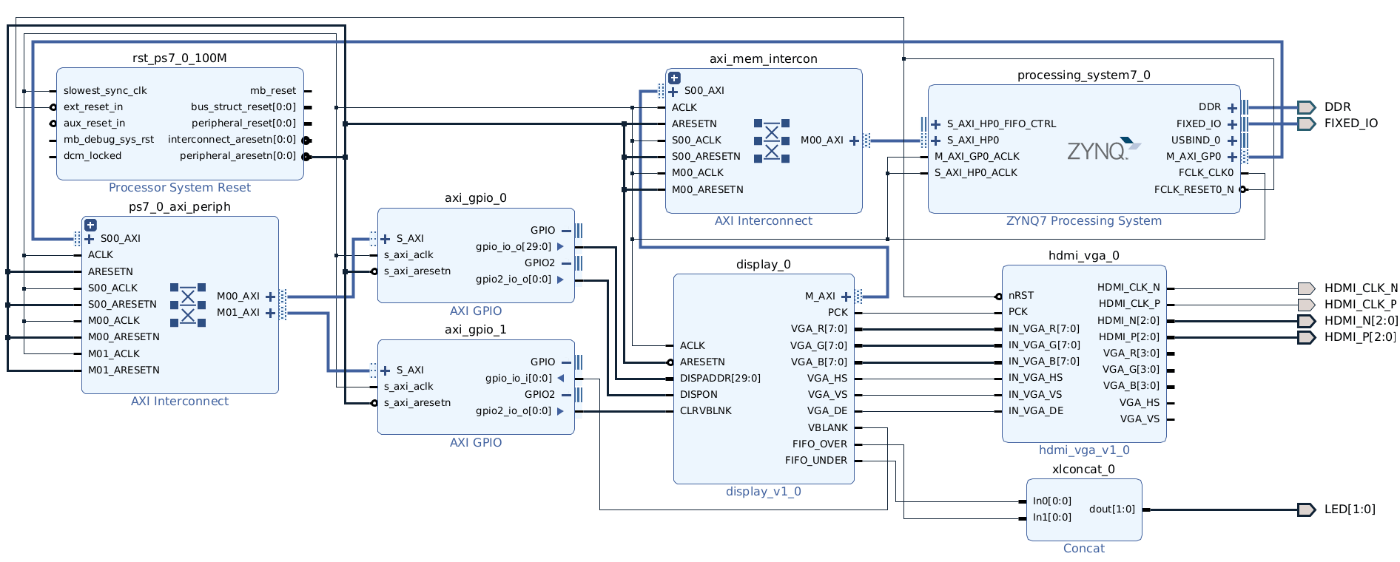
Designing the Graphic Display Circuit
- Create a new project
- Go to Tools → IP → Repository → Specify the directory of the previously packaged IP
- Also import the
HDMItoVGAIP in the same way - Create a Block Design
- Add Zynq PS
- Enable HP 0 for GPIO connection
- Clock Configuration → PL Fabric Clocks → Set
FCLK_CLK0to 100MHz - Run Connection Automation
- Add Display IP
- Run Connection Automation → Connect
M_AXIto Zynq through AXI Interconnect
- Run Connection Automation → Connect
- Add GPIOs for pixel address control
- Separate into 30-bit data output and 1-bit control signal output
- Prepare two GPIOs, both set to Dual Channel
- Specify the
S_AXIport and run Connection Automation
Something like this:

- Connect HDMItoVGA IP to the output of Display IP
- Create External Ports and rename them accordingly
- Validate Design
- Create HDL Wrapper
Block Design Completed
- Import constraint file
- Generate Bitstream
On-Board Verification
- Export Hardware
- Save TCL script (for Git management)
-
Launch Vitis IDE

- Create Application Project
- Use the
.xsafile from Export Hardware as the platform - Select Empty Application → Finish
- Import
disp_test.cintosrcof theDisplay_Circuit_Systemapplication - Build Project
Test Program Operation Check
- Variable settings omitted
- Code written in C
VBlank Wait
- Set
CLRVBLANKto clear the VBlank - Clear
CLRVBLANK - Hardware waits until VBlank becomes active
void wait_vblank(void) {
    XGpio_DiscreteWrite(&GpioBlank, CLRVBLNK, 1);
    XGpio_DiscreteWrite(&GpioBlank, CLRVBLNK, 0);
    while (XGpio_DiscreteRead(&GpioBlank, VBLANK)==0);
}
Rectangle Drawing Function
- Function to draw a rectangle
- First
forloop draws the top and bottom borders - Second loop draws the left and right sides
void drawbox( int xpos, int ypos, int width, int height, int col ) {
    int x, y;

    for ( x=xpos; x<xpos+width; x++ ) {
        VRAM[ ypos*XSIZE + x ] = col;
        VRAM[ (ypos+height-1)*XSIZE + x ] = col;
    }
    for ( y=ypos; y<ypos+height; y++ ) {
        VRAM[ y*XSIZE + xpos ] = col;
        VRAM[ y*XSIZE + xpos + width -1 ] = col;
    }
}
And finally, the main function does the following (roughly):
- Initialize display address and DISPON signal
- Initialize VBlank signal
- Call
wait_vblank - Set
Dispaddrto0x1000000 - Set
DISPONsignal active - Initialize all values in VRAM to 0 (write)
- Flush L1/L2 cache so values are reflected to DDR memory
- Use
drawbox()to write data into DRAM - When done, call
wait_vblankagain - Set
DISPONsignal inactive
Transfer to FPGA
- Connect Zybo board to PC and mount the USB port to WSL (this part is always tedious)
I usually run this from PowerShell, but if there’s a better way, let me know:
usbipd wsl list
usbipd wsl attach --busid <busid>
- Program the FPGA
- Debug As → Set breakpoints to verify the test program

Confirmed it works as intended
As usual, I’m skipping screenshots of the actual output from the FPGA because it’s a hassle to capture.