Article
Building a Hardware System with MicroBlaze
Introduction
Continuing from the previous post, this article documents the “Soft Macro CPU System” section from FPGA Programming Complete Guide, 2nd Edition.
My HDL background at this point was minimal. I had only spent about one day reading an introductory Verilog book and had learned only the basic syntax.
Environment
- FPGA: Xilinx Zybo Z7-20
- OS: WSL2 Ubuntu 20.04
- Development Environment: Vivado ML Edition 2022.1 for Linux
Objective
- Implement a hardware system equivalent to the one previously built with Zynq, but this time using the soft-macro CPU MicroBlaze.
- Because the UART communication path is already occupied on the Zynq PS side, direct PL-side communication is not available in the same way. Therefore, UART communication is handled through the MicroBlaze Debug Module.
What Is MicroBlaze?
- A soft-macro CPU provided by Xilinx.
- Supported bus types:
- LMB: for BRAM connections
- AXI: the ARM-style interconnect bus
- ACE: AXI extension
MicroBlaze Processor Reference:
Implementation
Hardware Construction
Build the hardware in Vivado:
Create Project → Create Block Design- Add the
MicroBlazeIP- Select
Microcontroller - Configure
Local Memory - Enable
Debug + UART - No interrupt controller is needed
- Select
- Run
Connection Automation
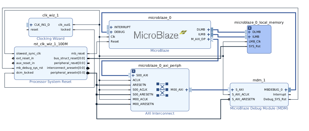
Peripherals such as local memory, clock, and reset are generated automatically.
Additional setup:
- Change the MicroBlaze input clock from
100 MHzto125 MHz - Since the
CLKpin is single-ended, change it fromDifferentialtoSingle End - Use reset as
Active High, and connect system reset and clock reset - Add a GPIO IP and use it as an
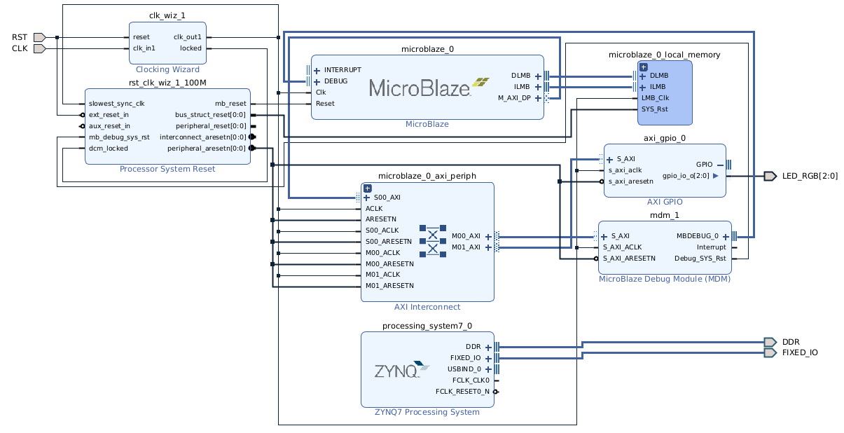
ALL Output [2:0], 1-channel configuration - Rename the I/O signal names to match the constraints file
- Finally, because an error appears otherwise, place the Zynq PS block as well
- Run
Validate Design → Create HDL Wrapper → Generate Bitstream
Final block design
When generating the bitstream, the following error appeared:
ERROR: [DRC NSTD-1] Unspecified I/O Standard: 5 out of 135 logical ports use I/O standard (IOSTANDARD) value 'DEFAULT', instead of a user assigned specific value. This may cause I/O contention or incompatibility with the board power or connectivity affecting performance, signal integrity or in extreme cases cause damage to the device or the components to which it is connected. To correct this violation, specify all I/O standards. This design will fail to generate a bitstream unless all logical ports have a user specified I/O standard value defined. To allow bitstream creation with unspecified I/O standard values (not recommended), use this command: set_property SEVERITY {Warning} [get_drc_checks NSTD-1]. NOTE: When using the Vivado Runs infrastructure (e.g. launch_runs Tcl command), add this command to a .tcl file and add that file as a pre-hook for write_bitstream step for the implementation run.
In short, the issue was that I/O assignments were missing, which caused the DRC error.
The cause was simply that I had forgotten to add the constraints file. After adding it, bitstream generation completed successfully, and I exported the hardware.
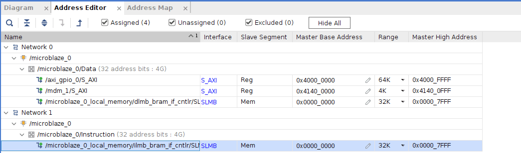
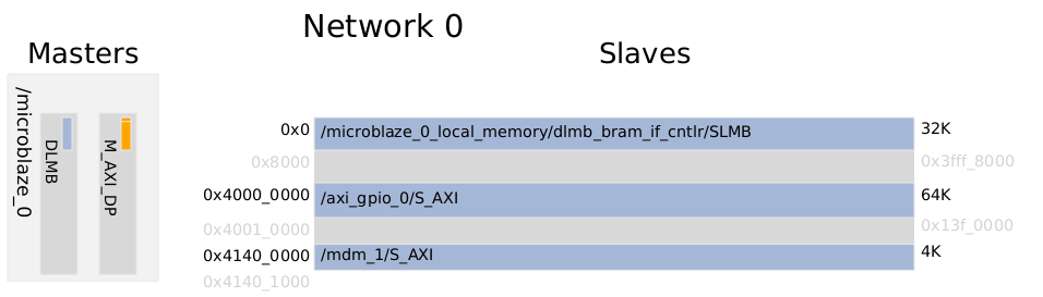
MicroBlaze address map
The register addresses for GPIO, BRAM, and MDM can be confirmed here:
Controlling MicroBlaze from Vitis
- Launch Vitis
- Create a platform project using the
.xsafile generated during hardware construction - Choose
Hello Worldas the application - Build the project
- Run
Debug As → Launch Hardware
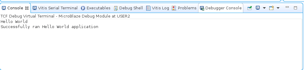
Execution completed successfully
MicroBlaze output is checked in the console through UART rather than through a normal serial port window.
Running an LED Control Program
Next, recreate the application project, control GPIO from MicroBlaze, and light the LEDs.
Import LED_test.c through Source → Build Project.
The code is based on the following publisher-provided reference:
/*xparameters.h
/* Canonical definitions for peripheral AXI_GPIO_0 */
#define XPAR_GPIO_0_BASEADDR 0x40000000
#define XPAR_GPIO_0_HIGHADDR 0x4000FFFF
#define XPAR_GPIO_0_DEVICE_ID XPAR_AXI_GPIO_0_DEVICE_ID
#define XPAR_GPIO_0_INTERRUPT_PRESENT 0
#define XPAR_GPIO_0_IS_DUAL 0
/*led_test.c */
#include "xparameters.h"
#include "xil_printf.h"

#define LED      *((volatile unsigned int*) (XPAR_GPIO_0_BASEADDR + 0x00))
#define LED_ctrl *((volatile unsigned int*) (XPAR_GPIO_0_BASEADDR + 0x04))

int main()
{
    int i, j;

    LED_ctrl = 0x0;
    xil_printf("Hello FPGA World!\r\n");
    while(1) {
        for ( i=0; i<5; i++ ) {
            xil_printf("i=%d\r\n", i);
            switch ( i ) {
                case  0: LED = 0x4; break;
                case  1: LED = 0x2; break;
                case  2: LED = 0x1; break;
                case  3: LED = 0x7; break;
                case  4: LED = 0x0; break;
                default: LED = 0x0;
            }
            for ( j=0; j<40000000; j++);
        }
    }

    return 0;
}
When Generate Bitstream is executed in Vivado, the hardware-side GPIO register definitions are generated in xparameters.h, and the control program accesses them through pointers.
From xparameters.h, we can see that XPAR_GPIO_0_BASEADDR reserves a 16-bit register space from 0x40000000 to 0x4000FFFF.
In operation, the while loop drives the 3-bit GPIO that corresponds to the three RGB LED outputs in the following order:
(100) → (010) → (001) → (111) → (000)
The pattern changes once every j < 40000000 delay loop.
What I Plan to Do Next
Run a design that combines MicroBlaze with a custom IP block. I may add that to this article later.
Impressions
- The AXI bus is extremely convenient.
- With this setup, I can perform control even without relying on the Zynq PS.