Article
Designing a Character Display Circuit and Custom IP with Vivado
Introduction
Continuing from the previous post, this article documents the “Pre-verification and Hardware Validation of a Character Display Circuit” section from FPGA Programming Complete Guide, 2nd Edition.
As a continuation of the previous article, I designed a character display circuit, packaged it as an IP block, and prepared it to run on FPGA hardware.
Environment
- FPGA: Xilinx Zybo Z7-20
- OS: WSL2 Ubuntu 20.04
- Development Environment: Vivado ML Edition 2022.1 for Linux
Objective
Create a circuit that displays characters on a monitor through HDMI.
Character Display Circuit Specification
- One character is composed of an
8 x 8dot matrix - Up to 80 characters horizontally and 80 lines vertically can be displayed
- VRAM is used to store character codes and character colors
- CGROM is used as a read-only memory that stores character patterns
Implementation
Project Creation
Project Creation → Create and Package New IPPackage a Specified Directory- Select the
chardisp_ipdirectory from the appendix and clickFinish
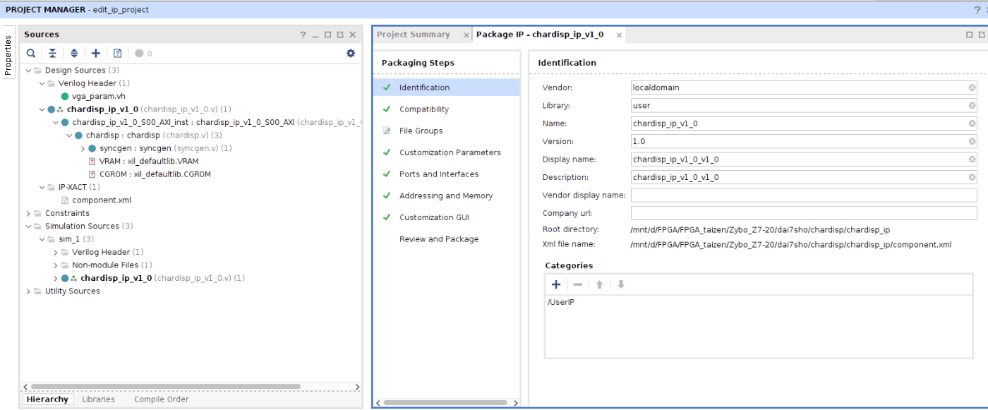
At this stage, VRAM and CGROM are still missing.
Generating VRAM
- Add the
Block Memory GeneratorIP - Customize the IP
- Memory Type:
True Dual Port RAMTwo ports are required because one side is used for display-timing reads and the other side is used for CPU read/write access through the AXI bus. - Byte Write Enable:
ON - Byte Size:
8 bitsThe VRAM data width is 24 bits, but this allows writes in 8-bit units. - Port A/B:
- Write/Read Width:
24 bits - Write/Read Depth:
4096
- Write/Read Width:
- Enable Port Type:
Always Enabled
- Memory Type:
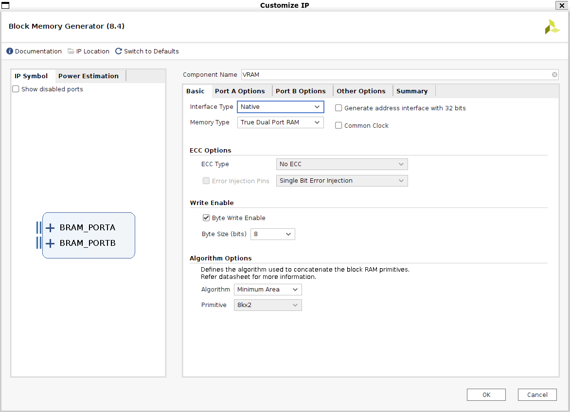
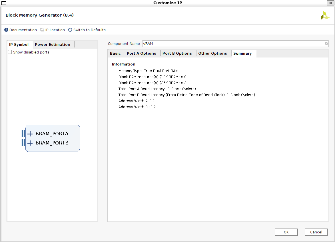
Check the summary and click OK.
- Run
Out of Context per IP → Generateto create the VRAM block.
Generating CGROM
- Add the
Block Memory GeneratorIP - Customize the IP
- Memory Type:
Single Port ROM - Port A Width:
8 bits - Port A Depth:
1024 - Enable Port Type:
Always Enabled - Other Options / Memory Initialization: enable
Load Init File - Select the
.coefile (CGDATA.coe)
- Memory Type:
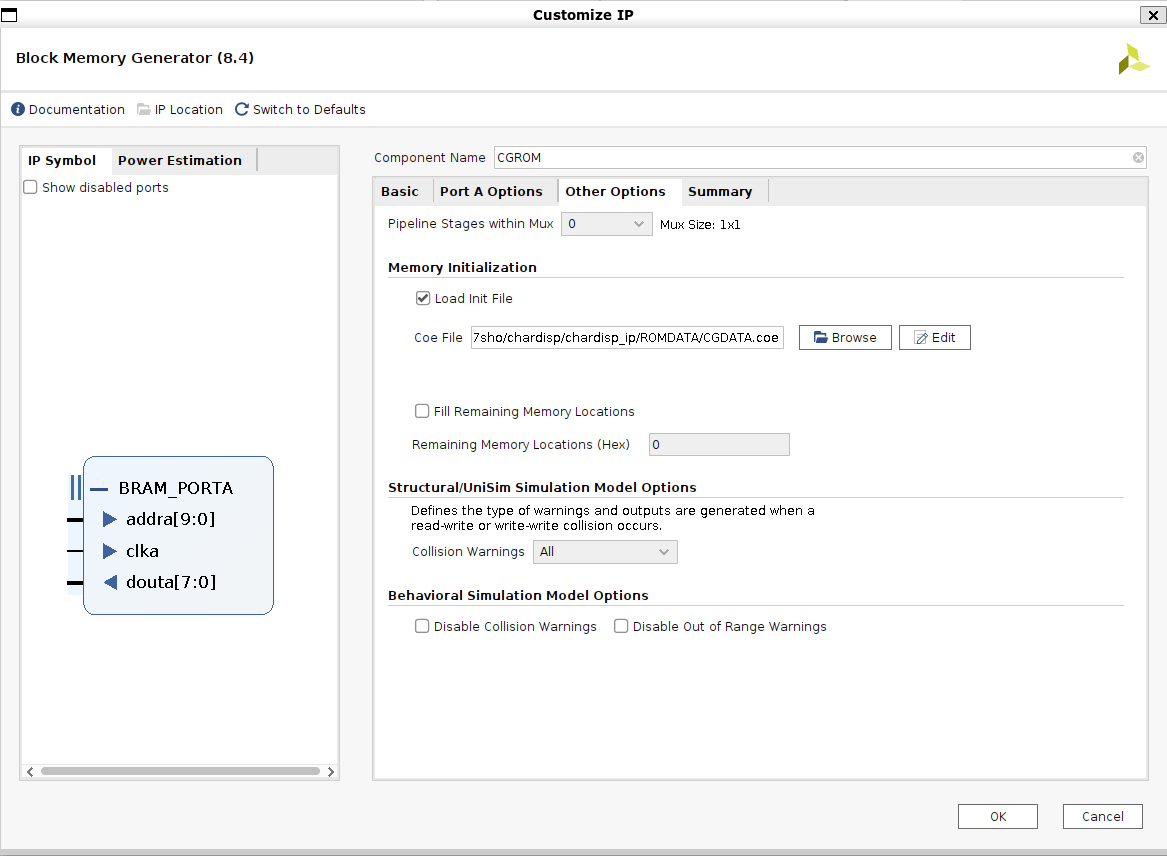
Check the summary and click OK, then generate the block.
Re-Packaging the IP
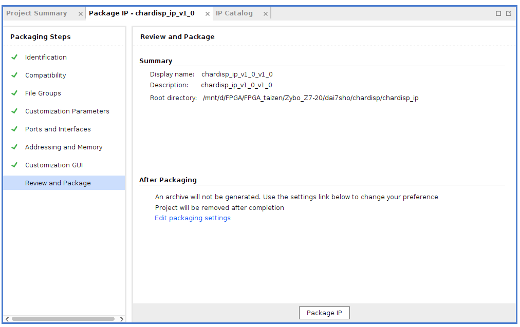
At this point, the character display circuit IP is complete.
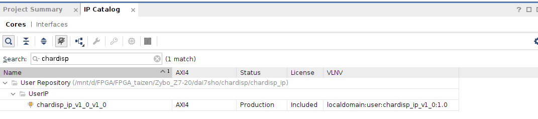
Now chardisp_ip can be called from the IP Catalog.
Simulation of the Character Display Circuit
- Create a new project for simulation
- Create a test bench that writes values into memory and outputs a file
- The overall procedure is the same as the earlier pattern display circuit design
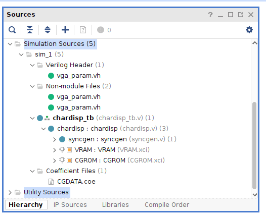
If the hierarchy looks like this, the setup is OK.
Run Simulation
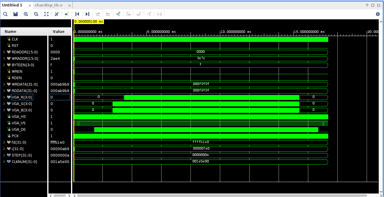
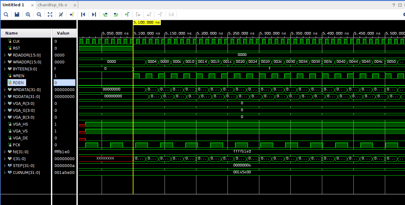
At 5.1 us, reset is released, write enable goes high, and data seems to be fetched from the CGROM.
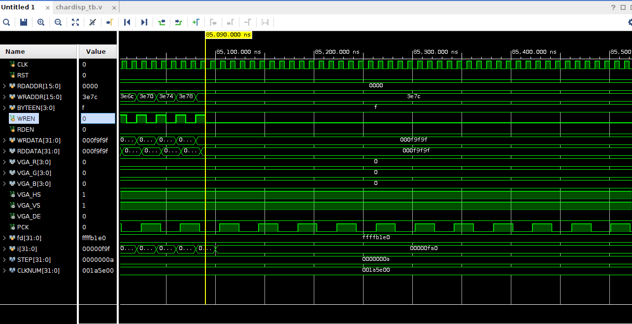
Around 0.85 ms, the memory write data has completed.
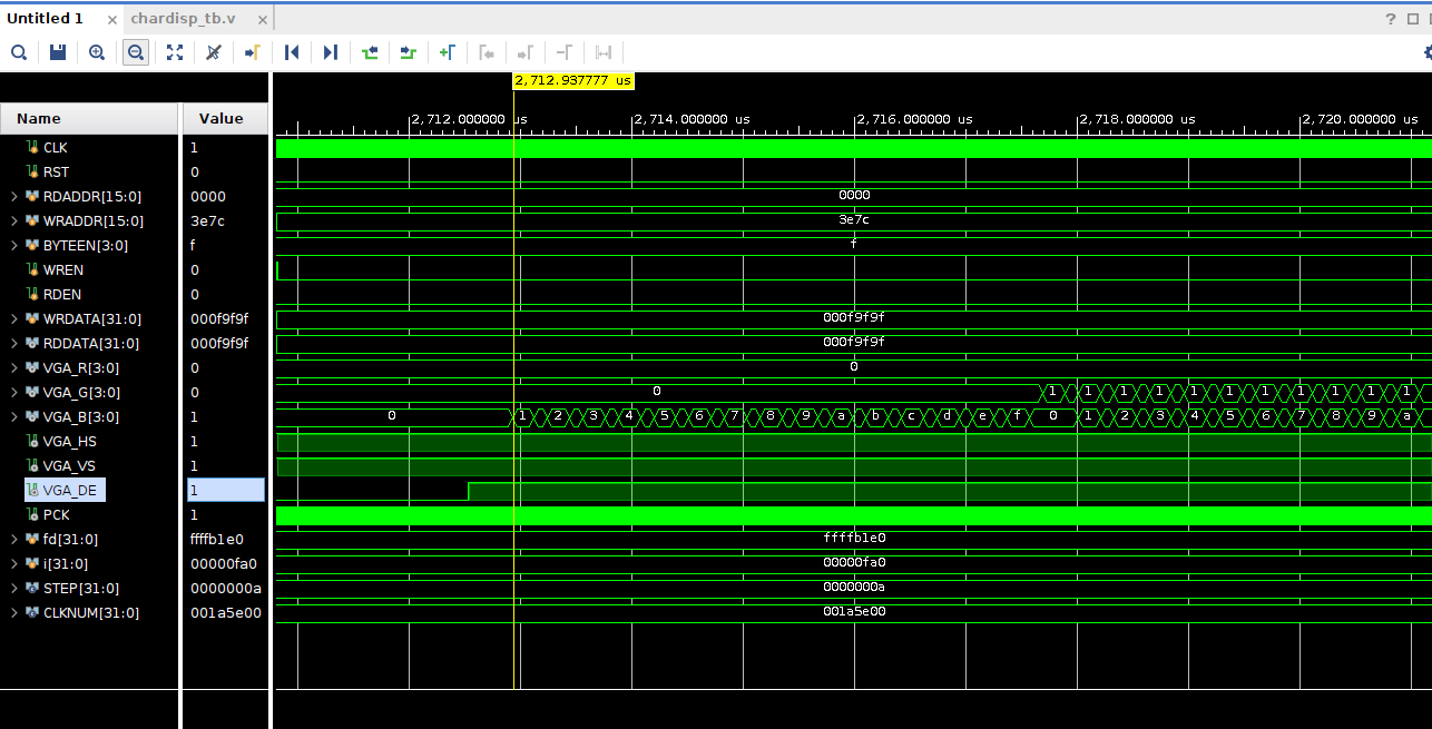
After VGA_DE goes high, RGB logic begins changing around 2.7 ms, which shows that the image is being displayed as intended.
Check the written data with IrfanView:
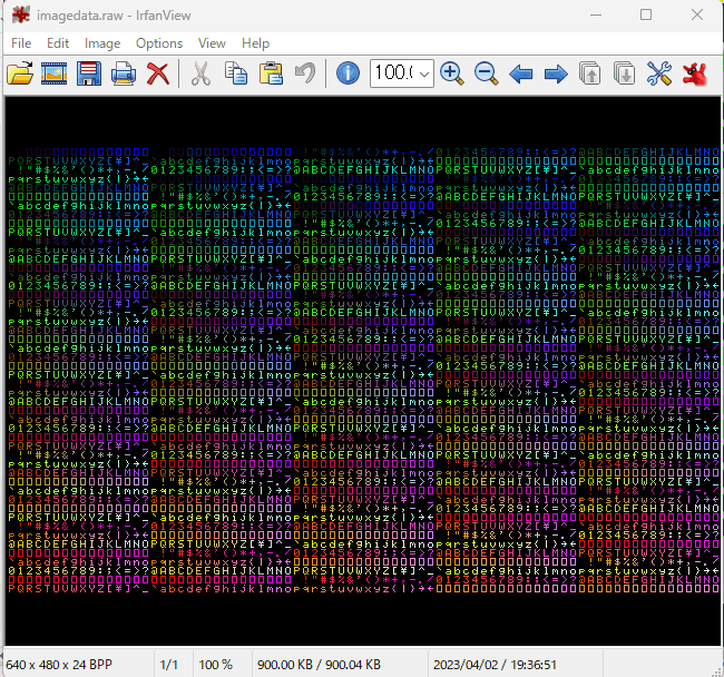
Simulation completed successfully.
Next Step
The next step is hardware validation on the actual board.