Article
Designing a Custom IP Block with Vivado
Introduction
Continuing from the previous post, this article documents the “Basic IP Creation” section from FPGA Programming Complete Guide, 2nd Edition.
In this post, the goal is to create a custom IP block with Vivado and integrate it into a larger hardware design.
Environment
- FPGA: Xilinx Zybo Z7-20
- OS: WSL2 Ubuntu 20.04
- Development Environment: Vivado ML Edition 2022.1 for Linux
Objective
Create a custom IP block with Vivado and integrate it into a circuit design.
Implementation
Adding a New IP
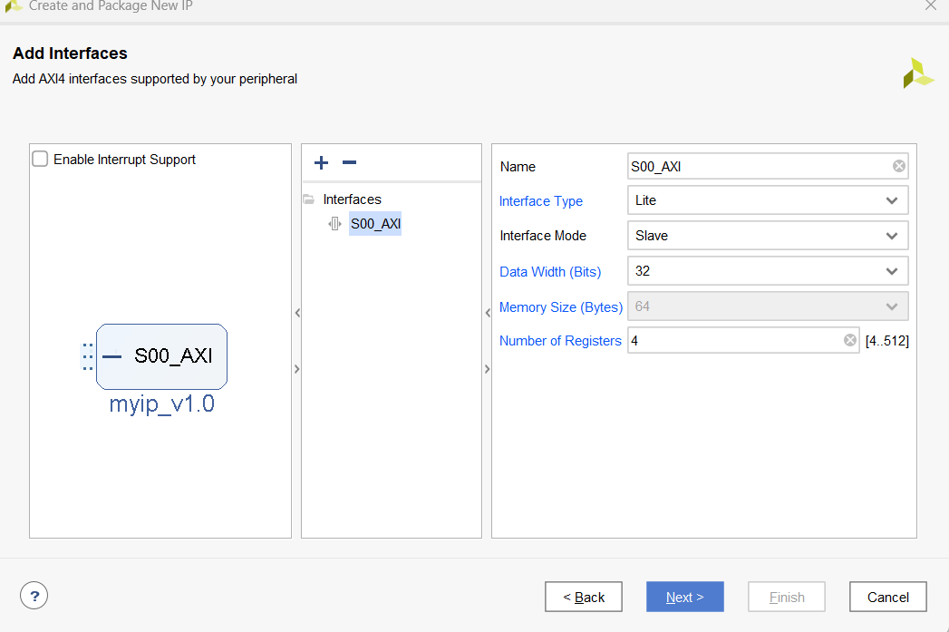
Tools → Create and Package New IPCreate a New AXI4 PeripheralNext Steps: Edit IP → Finish
About the AXI Bus
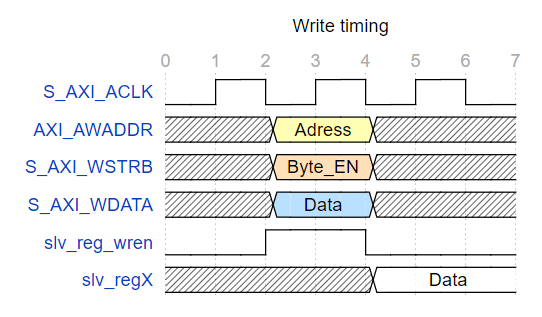
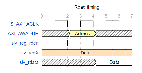
- AXI read and write channels are independent, so the register addresses
axi_awaddrandaxi_araddrare separated. S_AXI_WSTRBis a byte-enable signal that controls writes in 8-bit units.
Register Write Logic
always @( posedge S_AXI_ACLK )
	begin
	  if ( S_AXI_ARESETN == 1'b0 )
	    begin
	      slv_reg0 <= 0;
	      slv_reg1 <= 0;
	      slv_reg2 <= 0;
	      slv_reg3 <= 0;
	    end
	  else begin
	    if (slv_reg_wren)
	      begin
	        case ( axi_awaddr[ADDR_LSB+OPT_MEM_ADDR_BITS:ADDR_LSB] )
	          2'h0:
	            for ( byte_index = 0; byte_index <= (C_S_AXI_DATA_WIDTH/8)-1; byte_index = byte_index+1 )
	              if ( S_AXI_WSTRB[byte_index] == 1 ) begin
	                // Respective byte enables are asserted as per write strobes
	                // Slave register 0
	                slv_reg0[(byte_index*8) +: 8] <= S_AXI_WDATA[(byte_index*8) +: 8];
	              end
This code performs data writes to slave register 0 (slv_reg0) through the AXI protocol. When the target address is 2'h0 (that is, when the selected address bits are 00), the write operation is applied to slv_reg0.
case ( axi_awaddr[ADDR_LSB+OPT_MEM_ADDR_BITS:ADDR_LSB] )
This statement determines which slave register receives the write data based on the write address axi_awaddr. ADDR_LSB and OPT_MEM_ADDR_BITS are used to select the relevant address range.
for ( byte_index = 0; byte_index <= (C_S_AXI_DATA_WIDTH/8)-1; byte_index = byte_index+1 )
This loop processes the data width C_S_AXI_DATA_WIDTH in byte units (8 bits). The parameter defines how much data can be written at one time. It is typically 32 bits, although other widths are possible.
if ( S_AXI_WSTRB[byte_index] == 1 )
This condition uses the AXI write strobe signal S_AXI_WSTRB to choose which byte positions are actually written. The strobe acts as a bit mask: valid bytes are marked with 1, and only those bytes are updated.
slv_reg0[(byte_index*8) +: 8] <= S_AXI_WDATA[(byte_index*8) +: 8];
This line writes the corresponding byte of S_AXI_WDATA into the selected byte position of slv_reg0. The +: operator is a part-select operator used here to select the relevant bit range.
Register Read Logic
	// Implement memory mapped register select and read logic generation
	// Slave register read enable is asserted when valid address is available
	// and the slave is ready to accept the read address.
	assign slv_reg_rden = axi_arready & S_AXI_ARVALID & ~axi_rvalid;
	always @(*)
	begin
	      // Address decoding for reading registers
	      case ( axi_araddr[ADDR_LSB+OPT_MEM_ADDR_BITS:ADDR_LSB] )
	        2'h0   : reg_data_out <= slv_reg0;
	        2'h1   : reg_data_out <= slv_reg1;
	        2'h2   : reg_data_out <= slv_reg2;
	        2'h3   : reg_data_out <= slv_reg3;
	        default : reg_data_out <= 0;
	      endcase
	end

	// Output register or memory read data
	always @( posedge S_AXI_ACLK )
	begin
	  if ( S_AXI_ARESETN == 1'b0 )
	    begin
	      axi_rdata  <= 0;
	    end
	  else
	    begin
	      // When there is a valid read address (S_AXI_ARVALID) with
	      // acceptance of read address by the slave (axi_arready),
	      // output the read dada
	      if (slv_reg_rden)
	        begin
	          axi_rdata <= reg_data_out;     // register read data
	        end
	    end
	end
case ( axi_araddr[ADDR_LSB+OPT_MEM_ADDR_BITS:ADDR_LSB] )
As on the write side, the case statement branches using axi_araddr[3:2].
2'h0   : reg_data_out <= slv_reg0;
2'h1   : reg_data_out <= slv_reg1;
2'h2   : reg_data_out <= slv_reg2;
2'h3   : reg_data_out <= slv_reg3;
The selected slave register is assigned to reg_data_out.
if (slv_reg_rden)
  begin
    axi_rdata <= reg_data_out;     // register read data
  end
After that, when slv_reg_rden goes high, reg_data_out is transferred into axi_rdata, which becomes the AXI read output.
Modifying the IP
- Define output ports.
- Assign each defined
port[X:0]to the correspondingslv_reg[X:0]. - Add ports to the lower hierarchy and save.
Then run the following packaging flow:
Package IP → Packaging Steps → File Group → Merge changes from File Group Wizard → Re-Package IP
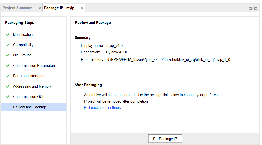
After reaching this point, add the IP from Create Block Design, generate the bitstream, and verify operation from Vitis.
Conclusion
- Confirmed the basic procedure for simple IP design.
- The next step is to integrate a custom IP block into the display circuit and execute it in the full system.